
This new transistor from China can put an end to Silicon’s reign and changes your next laptop into a speed demon
- Advertisement -

Related Posts
- Advertisement -
- Beijing University Transistor could perform better than Intel, TSMC and the best silicon chips from Samsung
- Full gate cover increases the speed and lowers energy consumption in breakthrough Chinese transistor design
- China may have just jumped American chip technology with this silicon -free transistor innovation
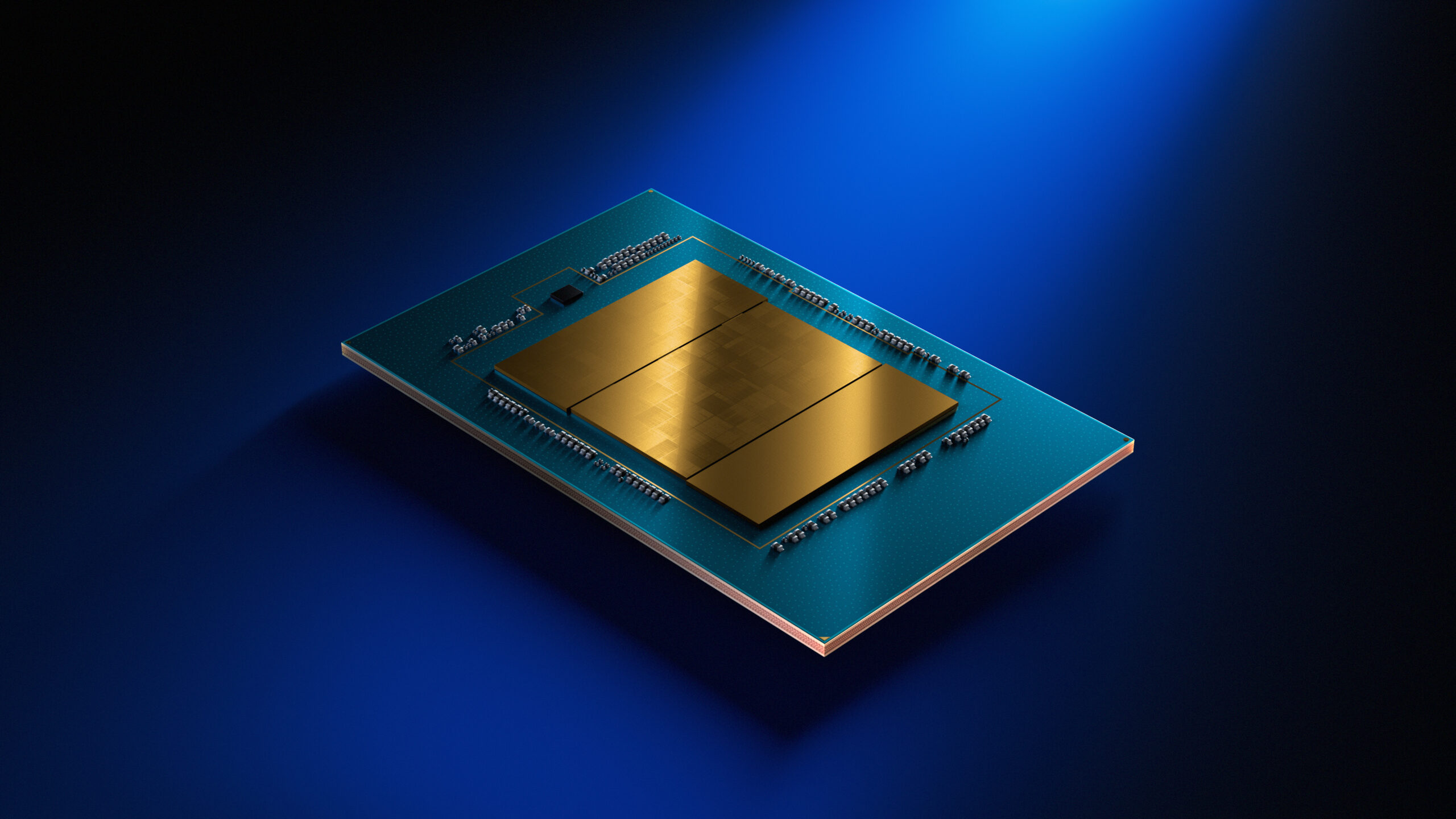
Chinese researchers at Beijing University have announced what a breakthrough in transistor design appears, which, if commercialized, could dramatically change the direction of the development of microprocessor.
The team created a silicon -free transistor based on a two -dimensional material, Bismuth Oxyselenide.
The innovation depends on the gate-all-around (cooled) architecture, where the gate of the transistor completely wraps around the source. Traditional Finfet designs, which dominate current silicone-based processors, all allow partial gate coverage. This full-wreat structure improves the contact area between the port and the channel, which improves performance by reducing the energy leakage and making better power control possible.
Could this mark the end of silicon chips?
Published in Natural materialsThe article suggests that the new 2D cooled silicon transistors can match or even surpass in speed and energy efficiency.
The researchers claim that their 2D transistor speeds have 40% speeds of speeds than IntelThe newest 3nm chips of 3 Nm while they use 10% less power, performance that it would place for the current processors of TSMC and would place Samsung.
The partial gate coverage in traditional designs limits the current control and increases energy loss. The new full-step structure treats these problems, resulting in high-voltage reinforcement and ultra-running power consumption. The team has already built small logic units using the new design.
“It is the fastest, most efficient transistor ever,” said Beijing University. These claims are supported by tests performed under identical conditions for those used for leading commercial chips.
“If chip innovations based on existing materials are considered a ‘shortcut’, then our development of 2D materials -based transistors is related to ‘changing lane’,” said Professor Peng Hailin, chief scientist of the project.
In contrast to the vertical structures of Finfets, the new design seems to be intertwined bridges. This architectural shift can overcome miniaturization limits with which silicon technology is confronted, especially because the industry pushes under the threshold of 3 Nm. It can also benefit the Fastest laptops that require such compact chips.
The team developed two new materials based on Bismuth: BIETE as the semiconductor and BIETSEO₅ As the gate dielectric.
These materials have a low interface energy that reduce defects and electrical scattering.
“This allows electrons to flow with almost no resistance, such as water through a smooth pipe,” Peng explained.
The performance results are supported by the DFT calculations (functional theory) of the density and validated by physical tests using a very accurate manufacturing platform at PKU.
The researchers claim that the transistors can be manufactured using the current semiconductor infrastructure, which simplifies future integration.
Maybe you like it too
- Advertisement -
